

|
|
|---|
| Links: Task 1: Theoretical & Experimental Study of Defects Task 2: Innovative Growth and Fabrication Processes for Defect Reduction Task 3: Evaluation of Defect Reduction Approaches and Device Applications Kickoff Documents (Restricted) 2011 Annual Review (Restricted) |
Task 2: Innovative Growth and Fabrication ProcessesTask
Leader: Yong-Hang Zhang (ASU)
Our team consists of several experts in the fields of MBE and MOCVD growth. We recently published results showing the first T2SL devices grown via MOCVD, a key to making them viable for widespread use. To improve the performance of T2SL IR detectors we will work on several new techniques to reduce the appearance of defects in devices grown in both MBE and MOCVD. This work will include:
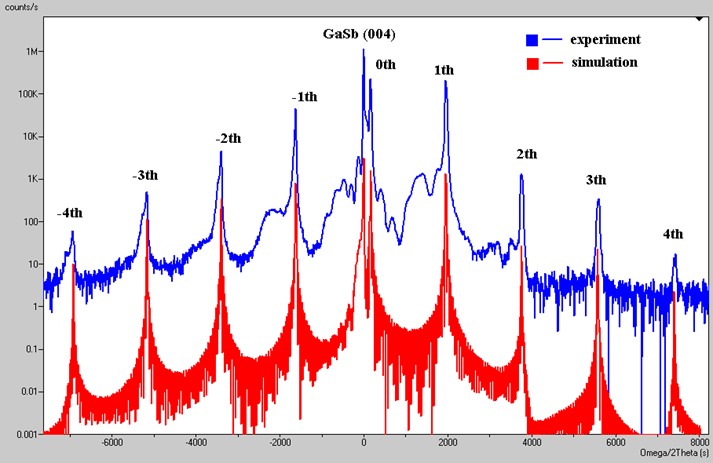 XRD pattern for the 100-period InAs/InAs0.75Sb0.25 SL with a 10 µm bandgap designed by YH Zhang and grown by Dupuis using MOCVD (XRD by Dupuis, Georgia Tech). |